


HP Workstation Labs Tour in Ft Collins
September 2014 – Part of the announcement and briefing on the new HP Z series workstations was a tour of the labs and Level 3 technical support area for the workstations. The facility in Ft Collins has a long history – nearly 30yrs of building workstations, high performance computing stations and customized graphics accelerators including high performance graphics ICs. As a result, being a system design and integration facility for the new workstations has a different look and feel from most computer manufacturers.
The tour started with the R&D Area which is focused on reliability and compatibility testing. Their setup includes multi-thermocouple testing (in some cases over 80 on a board) for thermal analysis and performance & compatibility analysis with memory, disk drive, optical drives, graphics cards, network cards, and other PCIe interface cards such as the SSD cache and storage devices. This area is located adjacent to the Level 3 Tech support, so if there are customer questions and issues, the techs have direct access to the design and compatibility folks who came up with the system to review the fix. This includes BIOS setting and modification for the motherboard and plug-in cards.
Moving from this area there is a number of system and board burn-in and environmental chambers that the units are tested in. A large number of applications have the workstations in a rack inside of an enclosure of a device (medical equipment and other equipment with large housings) that are subject to non-standard environments. These chambers not only test temperature high and low, but also humidity.
HP 10 Meter Chamber

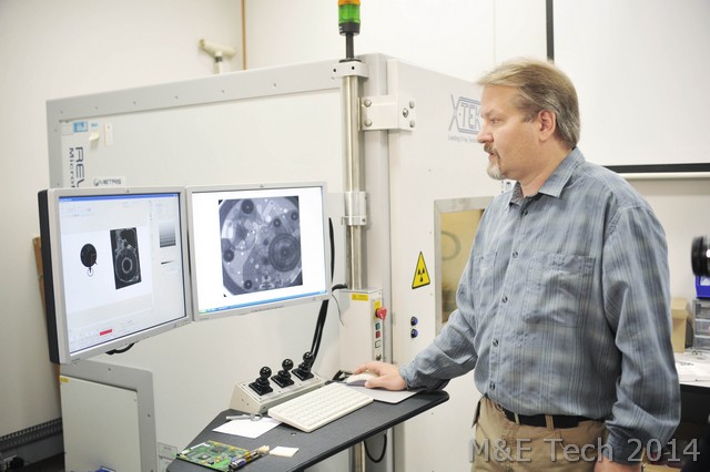
Two areas of the lab that are unique to have on site are the EMF testing with both a 10meter and a 3meter transmission room in-house. This in-house testing facility allows them to guarantee all the configuration options for the platforms instead of just the base configuration as most places do when they send the units out to test. The Lab also has an in-house material science lab. The lab features tensile and sheer stress testing, SEMs and other material level testing to be able to do detail failure analysis and incoming vendor analysis of the components. This is particularly key with the connectors on the plug-in cards. They are supposed to gold connectors of various thicknesses based on the speed and socket that the card goes in. In many cases it is a thin gold place over copper, and that impacts the performance of the system and the card. The analysis lab can do SEM images of these edge connectors and internal analysis of rotating media without disassembling the parts.
HP Material Science Lab at Ft Collins
Two stations are interesting to have on-site are the package test and model shop. The package test has shakers, drop test and bounce test machine to simulate shipment by air, truck and handcart. They test that the packaging supports the units without damage from up to a 6ft fall, and a several hour bumpy truck ride. In addition the package test, there is an in-house model shop. This shop has traditional lathes, milling machines, drills, etc for model making and has added laser cutting/etching, a water saw, a computerized milling/cnc machine, 3D printers and casting stations for traditional molds. This allows the engineers to come up with an idea, and get a form factor correct prototype typically the same day which greatly enhances the variety and diversity of solutions that are tried to address the customers needs.
Images of the briefing and lab tour can be found at the M&E Tech gallery
