


Vitesse video transceivers
April 4, 2011, We talked to Juan Garza, product marketing manager at Vitesse about the release of a new product family that combines a number of components into a single chip. These products are geared towards the broadcast and production video industries and are optimized for 75 ? SDI systems terminated with BNC connectors.
As studios and broadcast stations continue the transition to digital formats, the SMPTE-based systems are migrating to 3 Gbps interfaces with upgrades to 10 Gbps in the future. These systems encompass all of the equipment in studios and video postproduction processing including cameras, switchers, recorders, routers, all the way through to the distribution end.
The challenge for many system operators is that the wall of connectors and cables is passive, in that it lacks capabilities for debug of individual lines and signal integrity management. With hundreds of channels, this amounts to thousands of components and innumerable points of failure. In existing architectures, each channel goes to a crosspoint switch matrix.
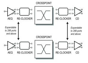
Standard video crosspoint swtich
All of the components are running at line rates, so everything scales with the number of ports. Power management becomes a major issue when this configuration is expanded out to hundreds of ports, as this can amount to hundreds of watts just for the interconnections between equipment. To make matters worse, there is no feedback or indicators for debugging a system problem, so testing requires manually checking individual ports.
To address all of these issues, they are announcing a new product family that integrates the send side and the receive side of the interface plus test capabilities. The testing is accomplished via an embedded waveform viewing function with diagnostics, and SMPTE pathological pattern generator on each chip.
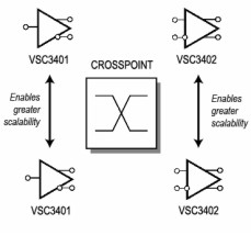
Vitesse Updated video crosspoint switch
The HDVScope is optimized for SDI and HD platforms and enables the operator to see the signal going to the cables. The integrated waveform viewer places a sampling test point at an I/O and collects data into a register. The data can be read out via an I2C port and viewed on a PC. The GUI allows the operator to view any input or output in the system.
As a result of integrating a waveform viewer into the chips, the operator can optimize send and receive signals and manage both systematic and random jitter, improving signal quality and integrity compared to other implementations. The reduced jitter margins permits longer cable runs or more open “eyes”.
These ICs reduce chip count, power consumption, and board space when compared to existing solutions. Fewer chips means fewer possible points of failure and higher reliability, especially important in the 24/7 working environment of a cable network studio. The inclusion of a pattern generator, BERT, and waveform viewer in every chip means that system debug becomes much faster and simpler.
The VSC3401 includes an adaptive cable equalizer with integrated re-clocker, and the VSC3402 is a video re-clocker with integrated cable line driver. Additional family members are the VSC3403, a quad input video re-clocker with cable line driver and the VSC3404, a quad re-clocker with integrated cable drivers. The parts will be on display at NAB in Las Vegas April 10-15
