


AMD shrinks design not process for Carrizo
February 2015 – At the ISSCC conference in San Francisco, AMD presented their latest APU architecture on their new processor codename “Carrizo”. The Accelerated Processing Unit (APU)is designed for notebooks and low-power desktop designs and features an advanced power management technology. It is expected that the Carrizo to reduce the power consumed by the new “Excavator” x86 CPU cores by 40 percent, while also providing substantial gains in CPU, graphics, and multimedia performance vs. the prior generation APU. The process also has a new generation of AMD Radeon™ GPU cores.
AMD new Carrizo High Density Library
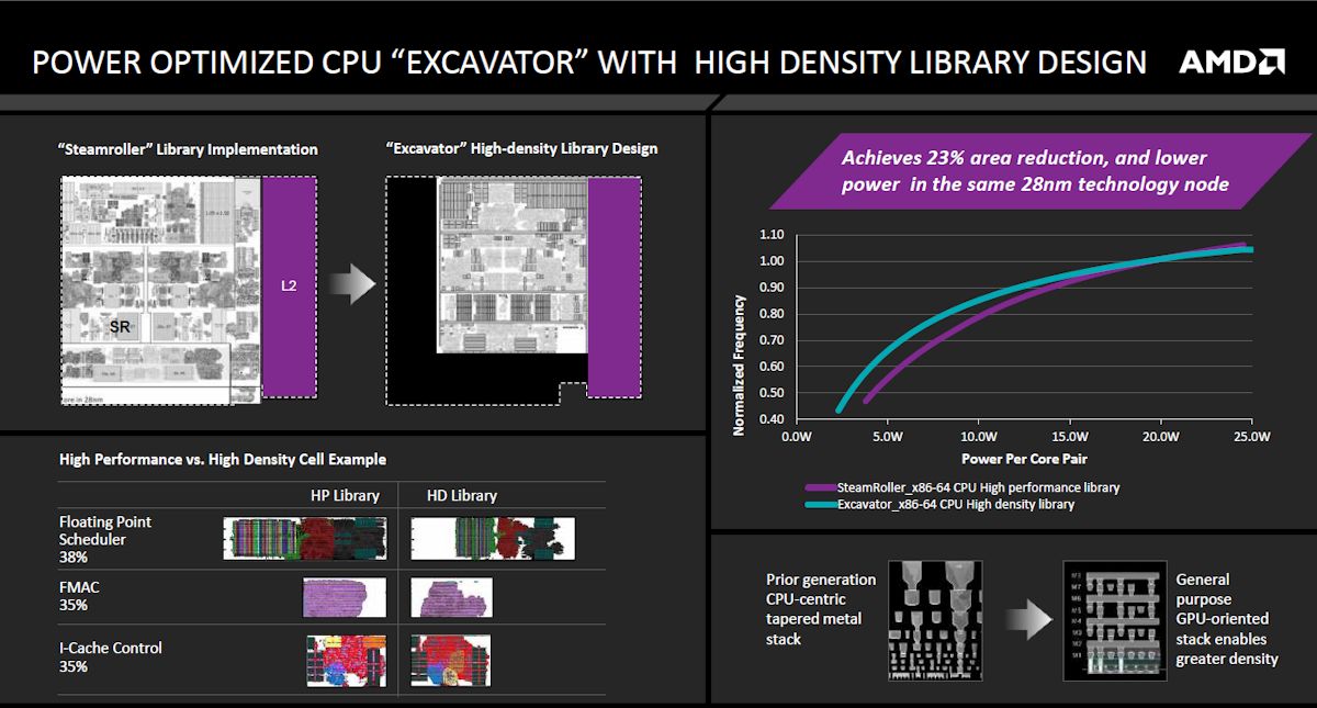
A major architectural change was the wiring interconnects and power grid separation on the new design. The GPUs now have separate power from the cores, and the granularity on the being able to turn off devices that do not need to be active has gotten finer so dynamic power down shuts off more devices. The new Radeon Graphics Core Next architecture brings support for Mantle, DirectX 12 and Dual Graphics. Like the rest of the chip, it is built using the new interconnect style.
These new high density design libraries allowed the Carrizo chip to fit 29 percent more transistors, 3.1 billion, in approximately the same die size as the previous generation, Kaveri APU built on the same 28nm process. This library redesign allows the current process node to be pushed to the next generation design, and have it be released this year, without needing a full process requalification. The extra space in the design allows for a larger graphics area, circuits for multimedia offload, and for the first time the integration of the “Southbridge” system controller on a single-chip. The multimedia offload includes the new video standard codec, H.265 which supports double the video compression of the H.264 engine and 4K resolution processing.
Space for more devices brought the integration of the Southbridge into the chip. This integration allows for the Carrizo to be the first processor in the industry designed to be compliant with the HSA 1.0 specification. The HSA compliance brings as a design advantage the heterogeneous Unified Memory Access (hUMA). With hUMA, the CPU and GPU share the same memory address space.
Further advancing the power technology is a technique AMD is calling adaptive voltage and frequency scaling (AVFS). This power technique uses new distributed sensors to monitor the actual in silicon speed and voltage sensors in addition to the traditional temperature and power sensors. These speed and voltage sensors enable each individual APU to adapt to its specific device characteristics, platform behavior, and operating environment in real time. By using this technique, the AVFS can provide up to 30 percent additional power savings.
These enhancements along with the continued use of the existing 28nm process technology, allows for quick introduction of these new processors into the marketplace. This introduction is targeted for 1st half of 2015, and being in products for holiday 2015.
